Schottky Diode Band Diagram
Schottky diode i v characteristics schottky diode is a metal semiconductor ms diode historically schottky diodes are the oldest diodes ms diode electrostatics and the general shape of the ms diode i v characteristics are similar to pn diodes but the details of current flow are different. Schottky diode band diagram.

Schottky Diode Definition Symbol Working And
It is recommended to read about the power diode classification and the difference between schottky diode and pn junction diode schottky diode basics.
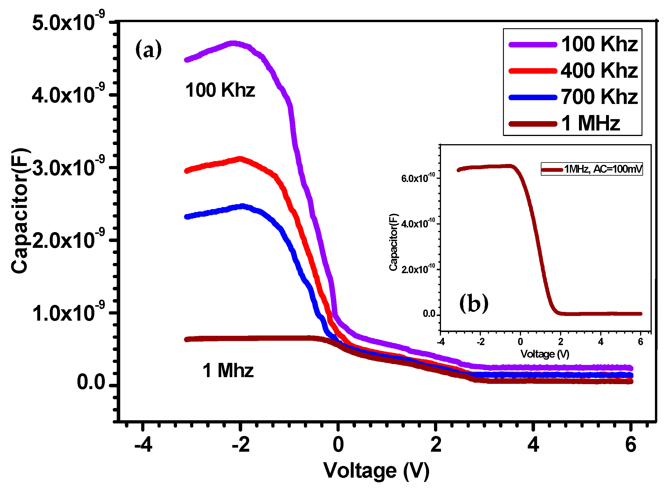
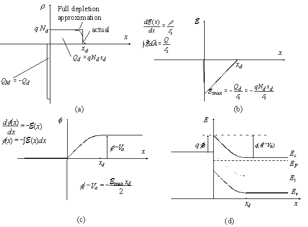
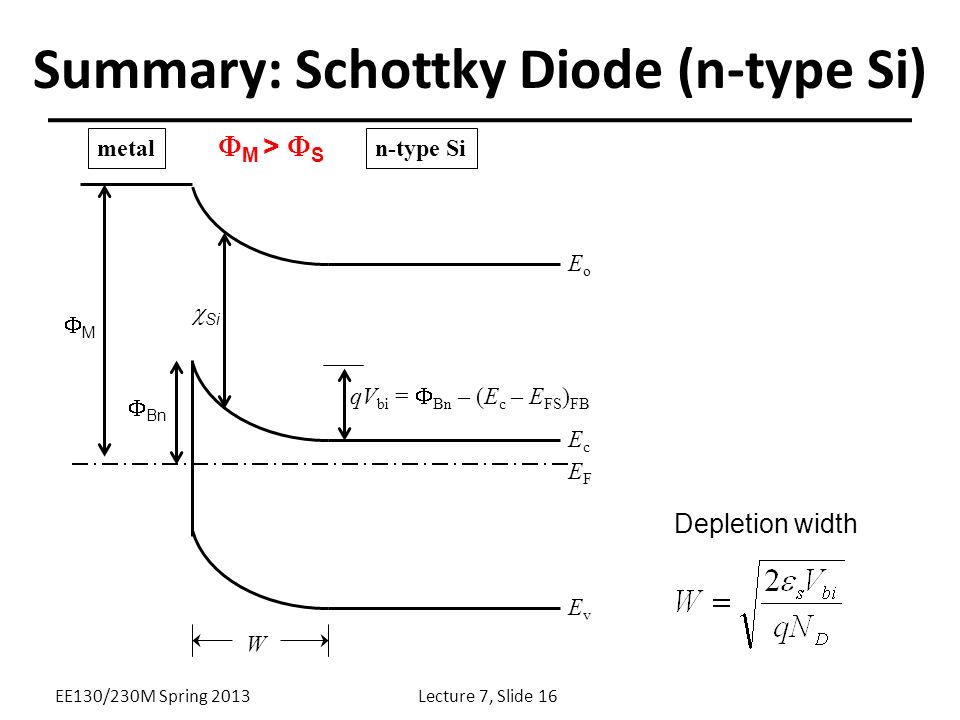
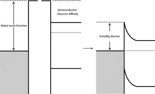
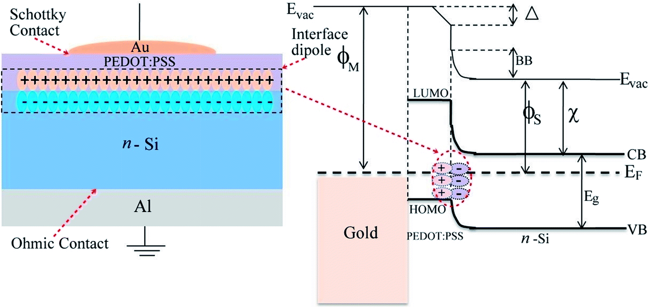
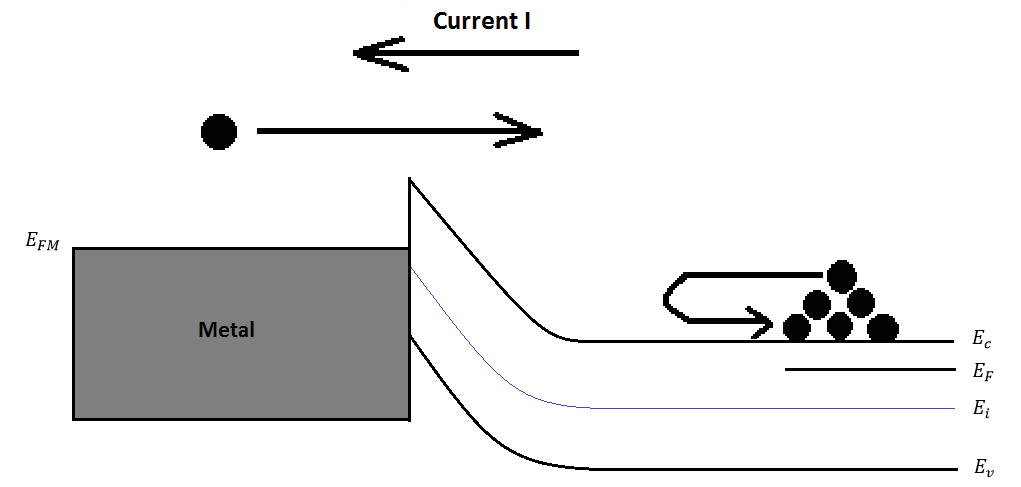
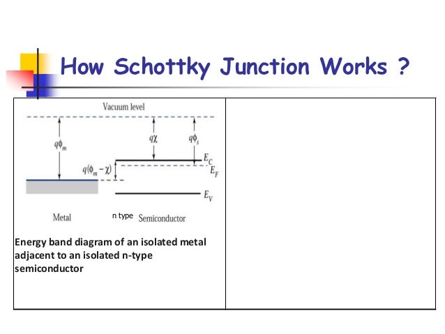
Schottky diode band diagram. Band diagram for n type semiconductor schottky barrier at zero bias equilibrium with graphical definition of the schottky barrier height f b as the difference between the interfacial conduction band edge e c and fermi level e f. Schottky diode sic based schottky diodes in this post let us discuss the schotttky diode is detail. A metal and n type semiconductor creates a barrier or depletion layer known as a schottky barrier.
For a p type schottky barrier f b is the difference between e f and the valence band edge e v. Schottky barrier diode is a majority carrier device of great. In a schottky diode the semiconductor band diagram looks very similar to that of an n type semiconductor in a p n diode compare fig.
Assume that interface states pin the fermi energy to. Schottky diode draw the band diagram valence band conduction band fermi energy for a schottky diode with a n doped semiconductor and a p doped semiconductor at zero bias. Schottky diode can switch on and off much faster than the p n junction diode.
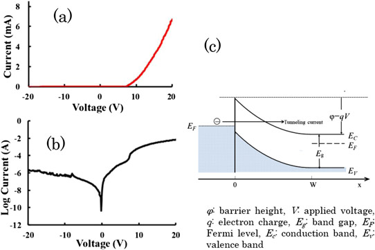
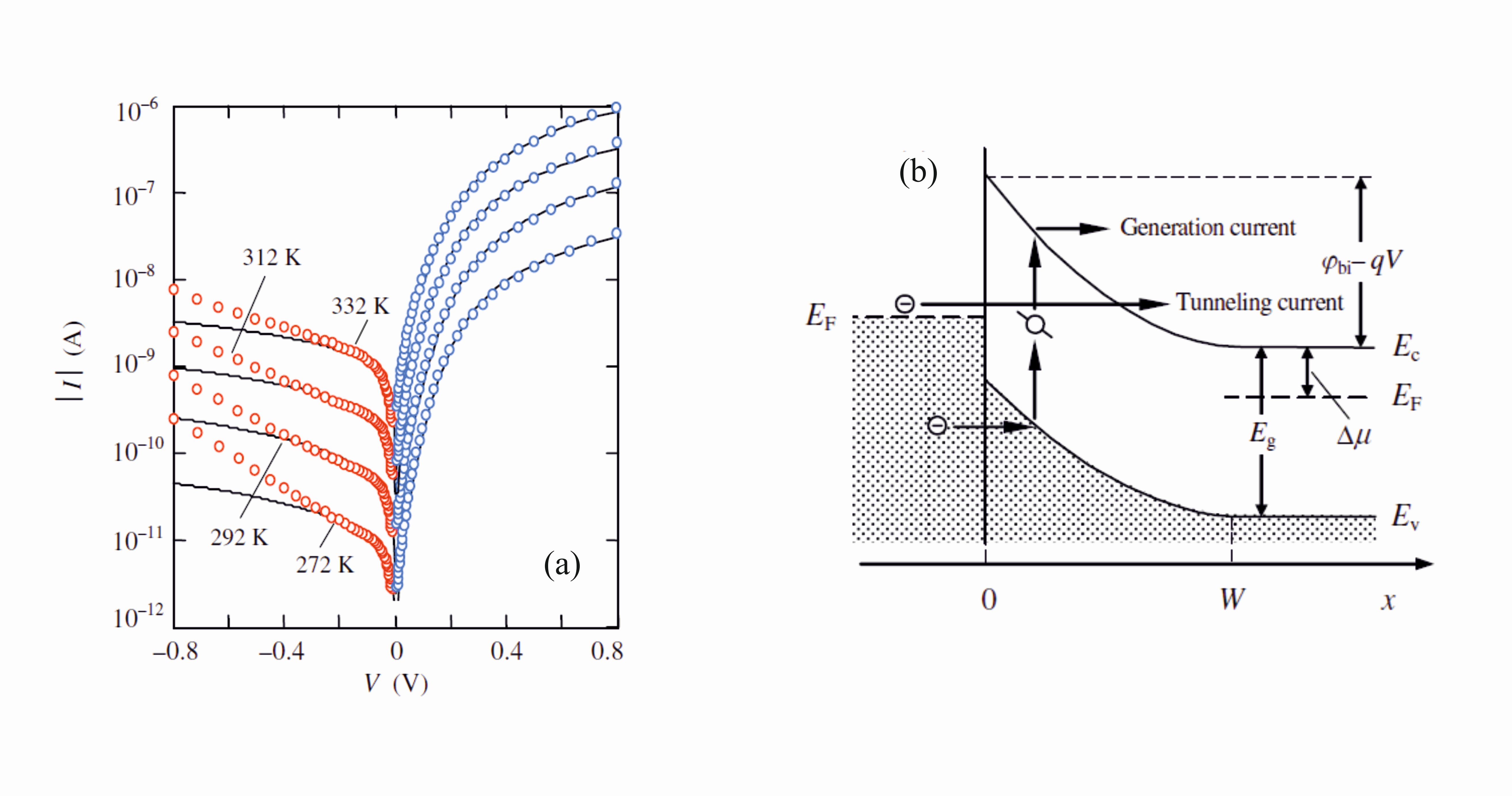
Energy band diagram of schottky diode. In solid state physics of semiconductors a band diagram is a diagram plotting various key electron energy levels fermi level and nearby energy band edges as a function of some spatial dimension which is often denoted x. Dominant currents in a pn diode.
Band diagram for schottky barrier at equilibrium. Schottky diode is named for its discoverer walter schottky. Importance of metal semiconductor junctions 2 equilibrium band diagrams 3 dc thermionic current simple derivation 4 intermediate summary 5 dc thermionic current detailed derivation.
Solid state devices lecture 17 schottkydiode gerhard klimeck. Schottky diode is a metal semiconductor junction diode that consumes less power than the p n junction diode.

Figure 1 From Modeling Aspects Of Current Calculation Of 4h

Figure 1 From A Micro Nuclear Battery Based On Sic Schottky
Schottky Diode

Schottky Diode An Overview Sciencedirect Topics

A Energy Band Diagram Of Back To Back Schottky Diodes With
1 Graphene Schottky Diodes An Experimental Review Of The

Microwave Diodes Why A Schottky Barrier Why A Point
Lecture 7 Outline Poisson S Equation Work Function Metal
Gan Based Schottky Diode Intechopen
Composition Analysis Of Two Different Pedot Pss Commercial
Coatings Free Full Text Electrical And Structural
Conductive Penetration Of Aluminium Nitride Buffers On

Schottky Diode Definition Symbol Working And
Description Of Transport Properties Of Schottky Diodes
Highly Non Linear And Reliable Amorphous Silicon Based Back

Schottky Diode
Metal Semiconductors Contacts Engineering Libretexts

Energy Band Diagram For A Schottky Diode On N Type Si Under
Metal Semiconductor Contact

Post a Comment for "Schottky Diode Band Diagram"